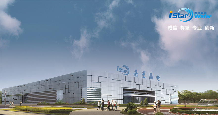
iStar Wafer Technology Co., Ltd. was founded in 2009. It is a national high-tech enterprise focusing on research and development of semiconductor materials, production of semiconductor equipment, and technology services etc.
The registered capital of the enterprise is 160.66 million yuan. It has an annual output of 12 million semiconductor substrate wafer production line.

What we can provide:
semiconductor materials
2~6 inch third generation compound semiconductor substrate wafers, including SiC, GaN, GaO.
Key semiconductor production equipment
Including semiconductor ingot slicing machine, wafer grinding machine, edge grinding machine, double side grinding machine, coordinate measuring machine, wafer surface inspection equipment, polishing equipment and other key production equipment.
Military products
Including radar photoelectric equipment window piece, missile fairing, military bulletproof glass, military semiconductor power communication devices, etc.
Materials used in Mini-LED, Micro-LED field
Including large size sapphire window development and production using in Mini-LED and Micro-LED

iStar Wafer keeps focusing on semi-conductive technology development, and accredit by Market and Government with our efforts.
iStar Wafer insists Honesty, Effort, Profession and Innovation, and keep focusing on semi-conductive area development. We aim to be recognized leader of semi-conductive material & equipment enterprise of Aisa.